Structures, Compositions and Fabrications of Microbump Based Interconnect Technology for High Density Packaging
This technology relates generally to multi-layer semiconductor devices. These devices are used in most of today’s electronics like phones, tablets, and computers. It is also useful in military applications for lightweight sensors and flight electronics.
Researchers
Figures
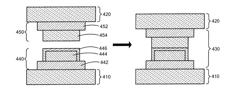
Interconnect with bump (top) and under bump metallurgy (bottom). The interface has a lower melting temperature than the bump and UBM due to the coated on low melt metal 446 which produces a corresponding fusible coupling surface 430
Simplified assembly for complex 3D architecture
Technology
This technology presents an approach to provide the thinnest possible active area cross section for a multi-tier, flip-chip capable, hybrid, 3D Integrated Circuit containing multiple SOI and non-SOI technologies. It uses microbump technology capable of creating single bumps for finer pitch structures or multiple bump arrays for larger pitch structures to minimize solder volume and spreading. The microbump technology minimizes the possibility of electrical shorts so the circuit is still functional. The interconnects consist of microbump and under-bump metallurgy where microbumps react with the under-bump at the interface to create a lower temperature melt interface. This interface melts at a lower temperature than the original bump materials, which makes it possible to create interconnects that can be reworked as double assembly and maintain reliable contact. These devices and circuit elements can be operated at low temperature to provide for reduced operating voltages, higher speed operation, and low power dissipation.
Problem Addressed
In the microelectronics industry, there is a trend toward the miniaturization of electronic devices, and consequently, a need for multilayer semiconductor devices. This trend also demands a simple and cost-effective assembly method for these devices, which include a combination of substrate and via structures. The multilayer devices must show that they can provide an increased circuit density compared to conventional semiconductor devices.
Advantages
- Minimized tendency to create electrical shorts
- Reduced Z-height, still capable of maintaining finer pitch interconnect, more efficient circuits
- Increased mechanical strength and stability at the interconnect
- Interconnects can be of various shape, size, and pitch at the same package level
Related Technologies
This case is related to MIT technologies: #17313, #16918, and #18705
License this technology
Interested in this technology? Connect with our experienced licensing team to initiate the process.
Sign up for technology updates
Sign up now to receive the latest updates on cutting-edge technologies and innovations.